At their most basic computational level, computers are made of some magical instruments: transistors are like the atoms that make all of matter around us, but for computers. They are the basic building blocks of all electronic components around us. Their use is so ingrained in our everyday lives, and yet, we don’t even know what they are. Well, not yet. Thankfully, you made it here.
Transistors are like astronomically tiny switches. They can exist as either zeros or ones, depending on whether a current flows through them or not.
They are made of materials called semiconductors. Semiconductors can be thought of as the middle ground between conductors – like metals – and insulators – like plastic, or wood. More technically, materials require free, or valence, electrons to actually conduct a current. How does these electrons come about? Every atom in the periodic table of elements – this crazy looking thing:
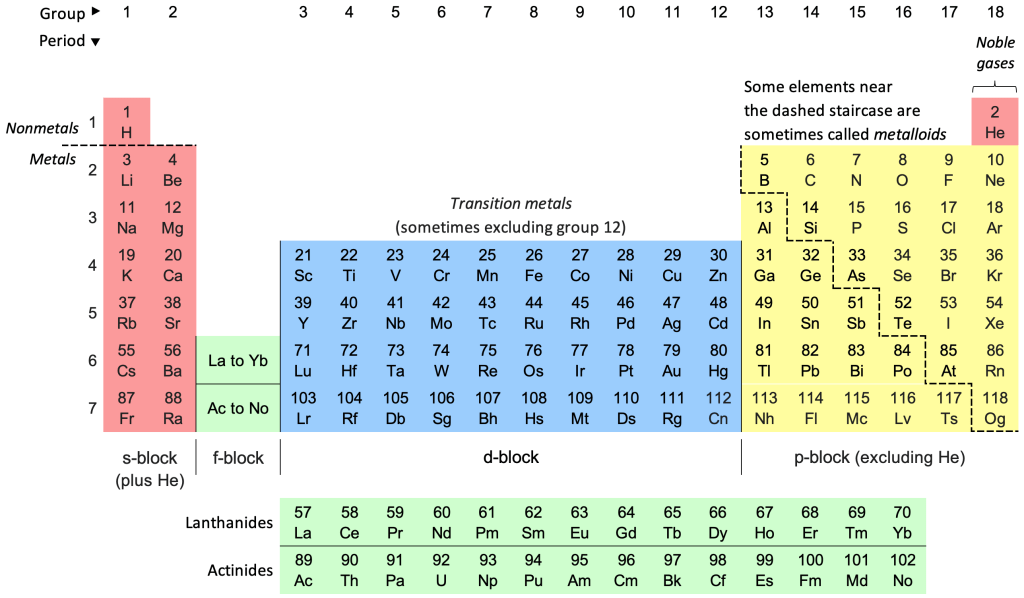
– has a particular structure. Take the He, or helium, atom for example:
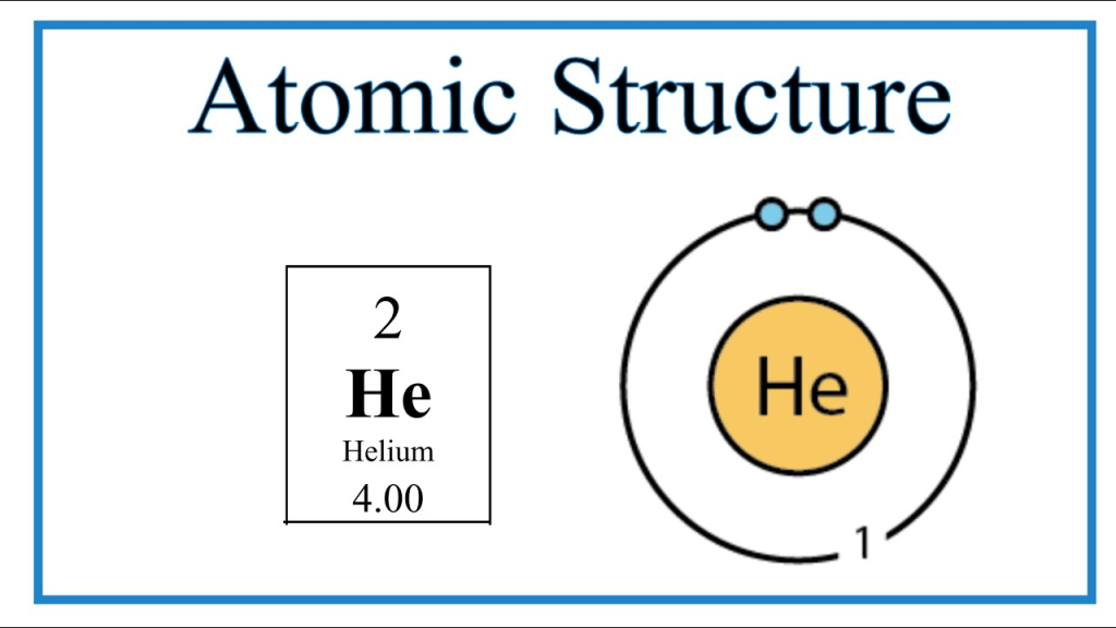
It has 2 electrons in the outermost shell. Any chemistry students in high school know that the first shell in an atom can have maximum 2 electrons. The second can have 8, third 18, and so on with the relationship 2n2, where n is the number of the subshell. What’s important here is that because it has filled up its outer shell, it does not have any valence electrons. Therefore, it cannot conduct electricity.
An atom like iron for example:
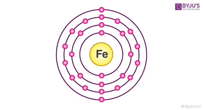
has 2 valence electrons making it an extremely good conductor, due to its mobile electrons.
Now, let’s talk about atomic structure more in-depth. Atoms with 4 electrons in their outermost shell can form bonds with other atoms through their electrons. If the other atoms also have 4 electrons, the atoms create a tetrahedral structure, like that of silicon:
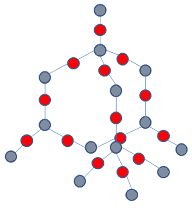
Since all the electrons are bonded, they cannot move around, hence the material is not able to conduct electricity. But, wait! Hold on. There’s a process called doping by which you can create mobile electrons, even in a tetrahedral non-conductive structure like silicon’s.
Doping refers to the addition of impurities to a substance to produce a certain electrical characteristic. Silicon, if doped by phosphorous, for example, becomes an n-type semiconductor. Wait wait. What happened?
When you “inject” phosphorous into the silicon structure, a small number of atoms – relative to the number of atoms of silicon – have an extra electron, since phosphorous has 5 electrons in its outermost shell. That is, 4 electrons are bonded by silicon atoms around it, with one being valence. This valence electron can be energised to move around the material.
Similarly, a material can be doped by atoms of 3 valence electrons, like boron. This creates a p-type semiconductor. While the material isn’t inherently positively charged, the “holes” it creates, due to 3 bonds with silicon and one non-bonded electron from silicon, acts like moving positive charges. Hence, the name p-type, or positive-type.
When these two types of materials are put together, some of the negative electrons from the n-type material move into the p-type material, filling the holes.
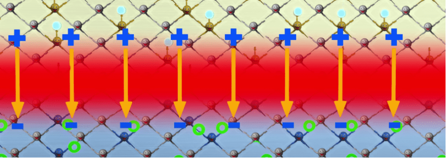
The above picture shows the formation of the depletion region (the red part), and a resulting electric field being created, going from positive to negative. Because like charges get repelled, the electrons can no more travel over the depletion region, because they get repelled by the negative “pole” of the p-type material.
This is where it gets interesting.
A transistor’s basic structure looks like this:
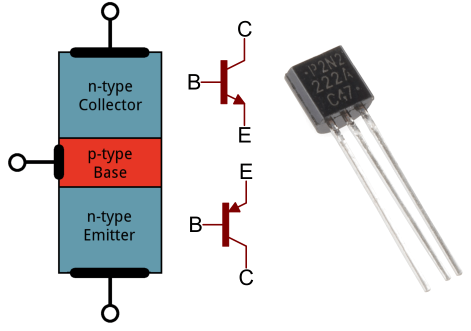
On the left we see that there are 2 n-type sides – one a collector and one an emitter – and more importantly, that a p-type material sits in the middle. On either sides of the n-type materials, a “source” and a “drain” is attached. The source is quite literally a source for electrons, basically a source for an electrical current. The current exits through the drain. Like said earlier, when put in contact with each other, n-type and p-type semiconductors create depletion regions, not allowing electrons to flow through.
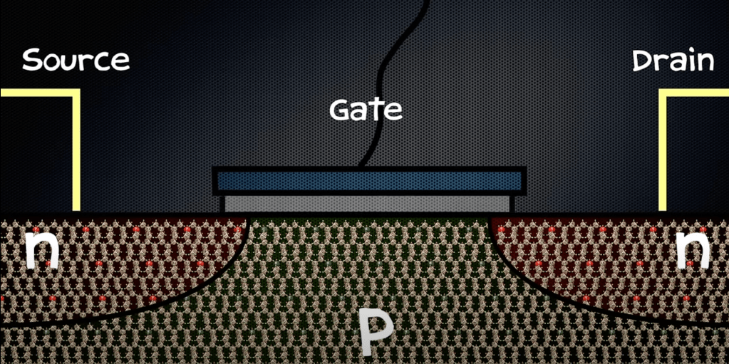
As seen above, a gate is attached to all the three materials. Currently, this transistor is the zero state. It does not have any electrical current passing through it. However, using the gate we can get it to its excited one state. The zero and one refer to binary digits in which computers communicate.
When the gate is switched on, it provides a constant positive charge to the p-type material. The important thing being that the positive charge is powerful enough to overcome the repulsion of the electrons and the negatively charged of the depletion layer. If it is, then the electrons travel through to the p-type material, and to the n-type material on the right. The motion can be summarised as follows:
Source -> n-type collector -> p-type semiconductor -> n-type emitter -> drain.
Transistors are so incredible tiny. In fact, they are only about 50 atoms across. They are so tiny, that sometimes electrons can actually tunnel through the barriers of the transistors and magically make it to the other side.
✨ Physics ✨
That’s for another time. I guess you’ll just have to keep reading.
Because I sometimes I struggle with this, every time I write a post I am going to write 3 things I am grateful for on the day I write the post:
- Indian food
- My ability to make decisions which positively affect my life
- My support system
Credits:
- https://en.wikipedia.org/wiki/Periodic_table
- https://www.youtube.com/watch?v=IcrBqCFLHIY
- https://www.youtube.com/watch?v=8k_-BRqO-Is
- https://www.shutterstock.com/image-vector/iron-atomic-structure-has-number-mass-1916962502
- https://byjus.com/chemistry/electronic-configuration-of-iron/
- https://www.chm.bris.ac.uk/motm/silica/silicah.htm
