In the previous post, we learned about how transistors are made. They’re made from semiconductors (middle in conductivity between conductors and insulators) and are extremely tiny. These transistors can be thought of as tiny switches. In other words, one can control the flow of an electrical current through a larger circuit by controlling the flow of the electrical current through the transistor.
This might sound spooky for many people unfamiliar with circuits. Many notations I will use are almost like alphabets for anyone familiar with circuit diagrams from high school Physics, but I will try to simplify it as much as I can. As always, you can reach out to me to ask questions, or just comment on this post down below. Now, to the meat of the post.
A transistor can be represented as a component in a circuit with the following symbol (excluding the colored arrows):
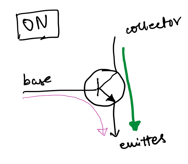
A transistor is an extremely interesting component, because, for the thick green arrow to exist, or in more technical words for the electrical current to pass through from the collector through to the emitter, a current must go through the base to the emitter. Looking at the diagram, the green arrow is only possible if the thin purple arrow exists. This is extremely important for the following development I will make.
A current through a transistor can pass from the collector to the emitter only if there is a current from the base to the emitter. Intuitively, a transistor can be thought of as a switch. Without the switch being turned on (or the current passing through the base to emitter), the current won’t flow (collector to emitter).
As mentioned in the previous post, “Yeah, but, what is a computer made of?“, transistors are the most basic components in computers. Think of them as the first floor to a building; without it everything else would break down. Just like any electrical circuit, you can connect transistors to any other electrical components, such as wires, batteries, cells (both are different: batteries are collections of cells), LEDs (Light Emitting Diodes), and many more. However, one can make extremely fascinating things if you connect transistors with other transistors.
Specifically, transistors in particular arrangements can form things called logic gates, which are “basic digital circuits that performs logical operations on binary inputs to produce a binary output.”
Firstly, let’s dabble with a simple transistor circuit.
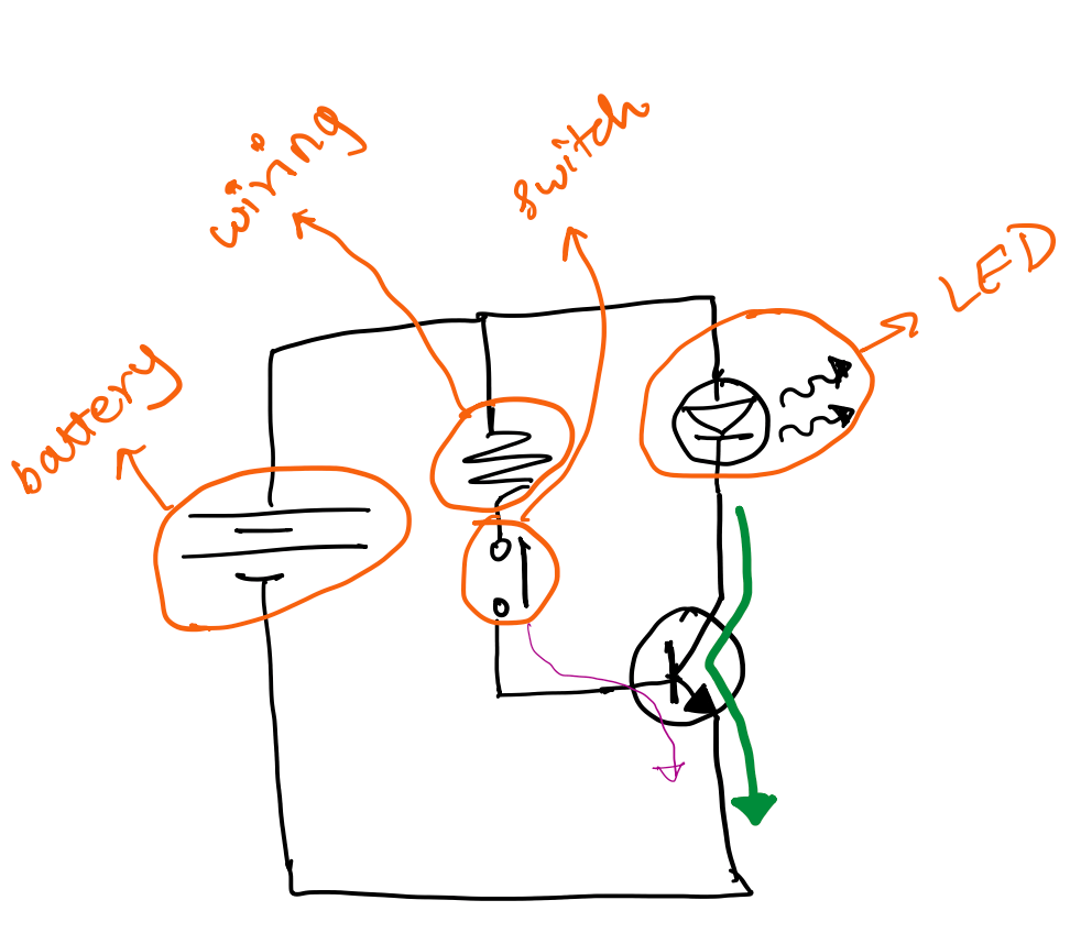
The above picture, drawn by yours truly, shows a transistor in a circuit with a battery, a switch, and an LED. All black lines indicate wiring, excluding the squiggly line, which indicates a resistor (while this is an important symbol, it does not play a crucial role in understanding our particular example). The purple thin arrow shows the current that needs to flow through the transistor to allow the big green arrow to flow. Contextualising the example, unless the current doesn’t flow through the base to the emitter (the purple arrow), the current indicated by the green arrow will not flow. Green dots are put at parts of the circuit called “junctions”; these are points where 2 or more wires connect, allowing current to split up.
In this case, one needs to press the button down to allow the current to flow from the base to the emitter, which in turn will allow the larger current to flow through the LED, which will light the LED up. We can control whether the LED will light up by placing a button in the circuit.
Now, let’s see a basic inverter logic gate.
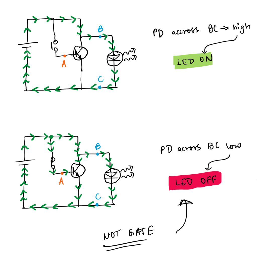
The first diagram above shows a current (indicated by the repeated green arrows) travelling across the circuit, through points B and C, and NOT through A. This happens because the button is not pressed, or as referred to more technically, the switch is open. When this is the case, the current doesn’t flow through point A, thus not going through the transistor. Therefore, the difference in potential across B and C is high, allowing the LED to light up.
In the next example however, since the switch is now closed, current can now pass through the transistor, eliminating the difference in potential that is required for the bulb to glow. Think of the potential difference as a necessary prerequisite for the bulb to glow. If that condition is not met, as in the second example, the bulb will not light up.
To revise, when the button is open, that is the input is zero (assuming not pressing down the button is considered “0” in the binary sense), the output in one (that is, the LED lights up).
When the input is one (the switch is closed), the output is zero (the LED does not light up because the potential difference prerequisite is not met).
You have just created an inverter circuit, also known as the “NOT” logic gate. To summarise our results rather simply, we can create a Truth Table. This explicitly states the outputs derived from certain inputs we feed the system. The input here was us pressing down the button or not.
| INPUT | OUTPUT |
| 0 | 1 |
| 1 | 0 |
Another simple to understand logic gate is an AND gate. It’s circuit diagram is:
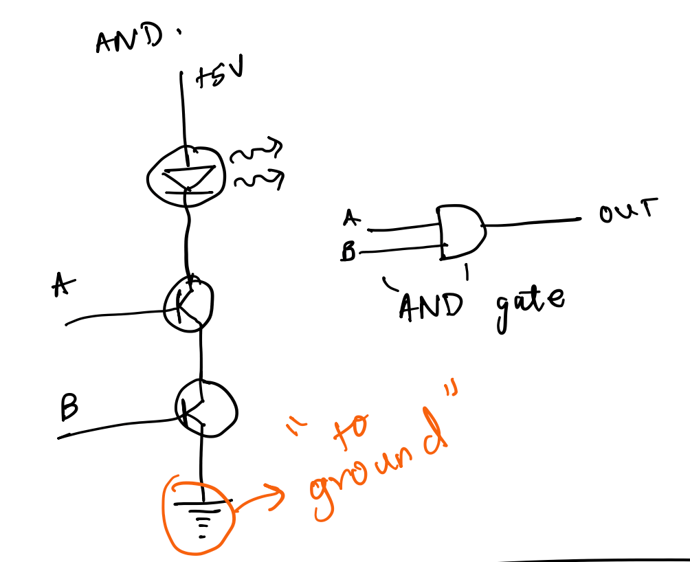
In this case, two transistors are connected in series, in which all circuit elements are arranged in a single path. Two inputs, A and B, allow us to control the state of the transistors and the LED. Feeding a current into the input A allows the larger current to pass through the first transistor.
The special property of this setup is that both inputs A & B must be “1” for the output to be one. In other words, both transistors must have a current running from their bases to the emitters for the larger current to flow from the LED to the “ground”. Some may wonder why the current must flow completely through the circuit for the LED to glow. There is a simple answer: electrical components only work if the circuit is complete. There can’t be one open end of the circuit because then the current can’t “flow”.
The Truth Table is:
| INPUT A | INPUT B | OUTPUT |
| 0 | 0 | 0 |
| 1 | 0 | 0 |
| 0 | 1 | 0 |
| 1 | 1 | 1 |
The Truth Table shows us that both A & B must be “1” for the LED to glow. This is known as an AND gate, denoted by the symbol in the photo.
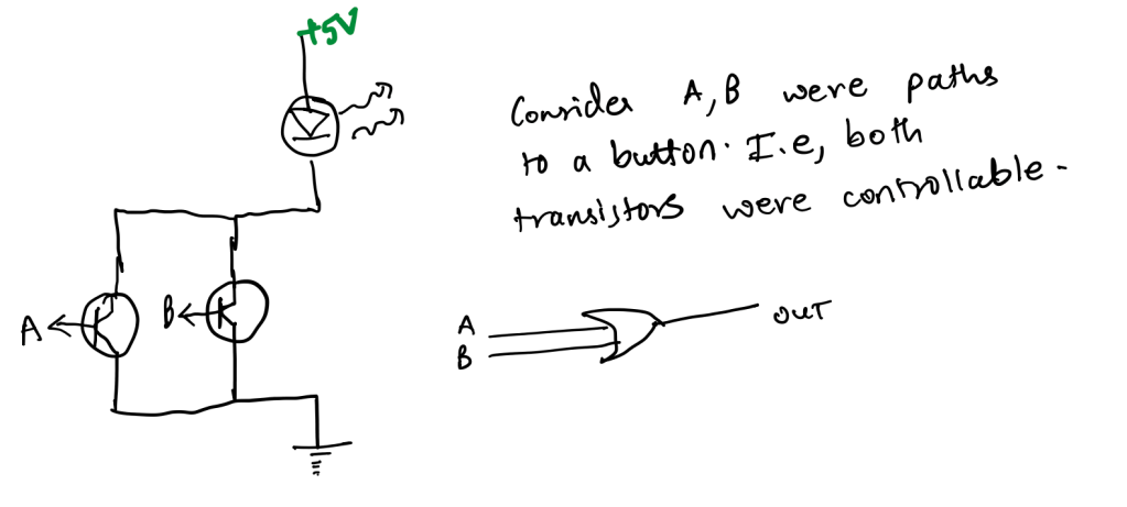
Take a second to think about all that you learned. For a little fun exercise, and a challenge, try to look at the following circuit diagrams and understand them yourself.
Circuit 1:
Truth Table:
| INPUT A | INPUT B | OUTPUT |
| 0 | 0 | 0 |
| 1 | 0 | 1 |
| 0 | 1 | 1 |
| 1 | 1 | 1 |
Circuit 2:
Truth Table:
| INPUT A | INPUT B | OUTPUT |
| 0 | 0 | 0 |
| 1 | 0 | 1 |
| 0 | 1 | 1 |
| 1 | 1 | 0 |
Maybe you understood circuit one, but you couldn’t give a damn to put in all the effort of understanding circuit 2. Don’t worry. Been there, done that.
Let’s revisit circuit 1. That shows a classic OR logic gate. By the name, one can intuitively understand it means that whether A or B are 1, the output will be 1. However, when both are zero, the output will be zero too. If A or B were 1, that is, a current was flowing from the base to the emitter, it would allow the current to pass through to the ground thus making the output “1”. This arrangement of transistors is known as a parallel arrangement.
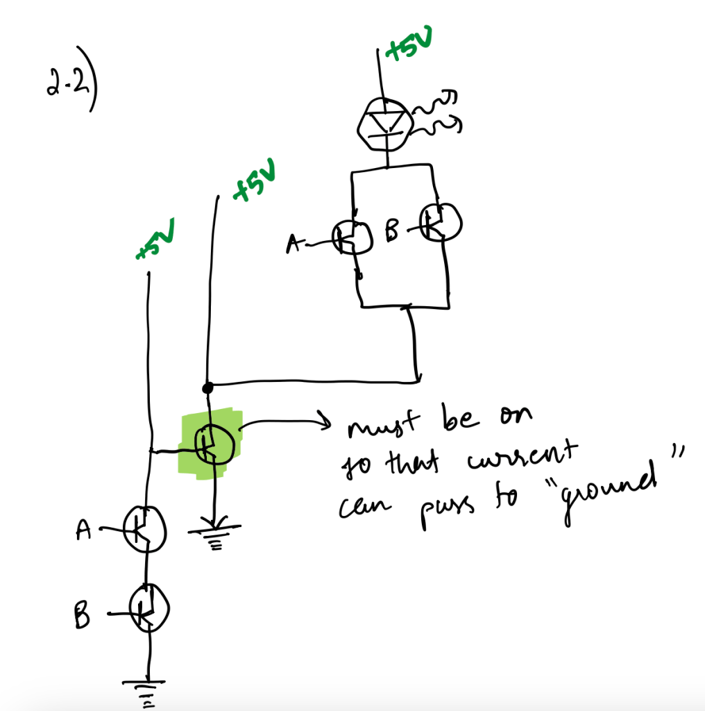
Now, the interesting one. Circuit 2. Maybe you noticed that the top right part of Circuit 2 is just the OR gate. However, the output of the OR gate is reliant on another part of the circuit. It might be easier to break the circuit up.
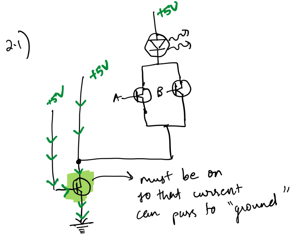
Eliminating the left-most series combination, we get a much simpler circuit to understand. This above circuit implies that the output – controlling whether the LED glows – is dependent on the transistor highlighted with green. That is, if the input from the OR gate is 1, the output can only be 1 if the transistor is ON. The transistor being ON depends on the left-most wire providing a current to the transistor. However, if there is a constant current being fed into the transistor, the Truth Table for the above circuit would just look like the OR gate.
To reach Circuit 2’s Truth Table, we need to control the input current into the base of the transistor highlighted green.
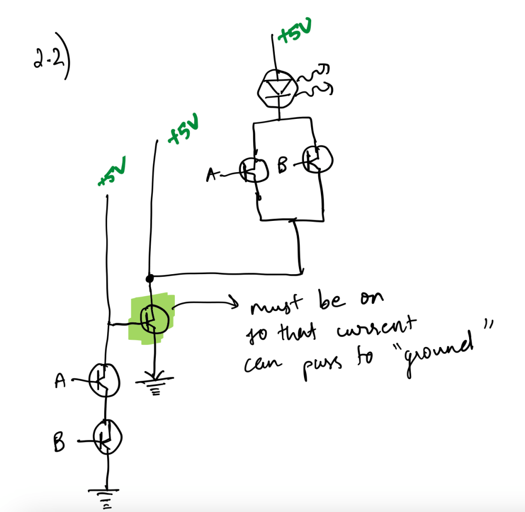
By adding two transistor on the left-most wire, we can control the flow of current to the green transistor. An important note is that both transistors are connected to the same inputs as the OR gate, A & B. Therefore, for this whole setup, there are only two inputs needed.
Let’s take the first case where both A & B are zero. Since no current passes through the OR gate, there is no possible output, therefore the output is just zero. The LED doesn’t glow. This was simple.
Always remember that our job is to control when the LED glows.
Now, let’s have A as 1 and B as 0. Since its an OR gate, when either A or B is 1 the current is allowed to pass, thus the current reaches the green transistor. However, this is not enough for the LED to glow. The circuit is not complete yet. When A is 1, the transistor on the left-most wire with the input A is turned on. However, the current cannot pass through the transistor with the input as B, because B is zero. This means that the green transistor has an input current from the base to the emitter, allowing the current to pass through to the ground on the middle wire. The LED glows. Hooray!
This is the same case with A as 0 and B as 1.
However, when both are 1, the left-most wire has both transistors turned ON, allowing that current to pass through, removing the input current into the green-highlighted transistor. This switches the green-highlighted transistor OFF, thus not allowing the output from the OR gate to pass, making the LED switch OFF.
This is quite a complicated circuit, even I took a couple tries to understand. Reading through it again could help you.
I know this was a rather text and logic heavy post, but I really enjoyed this topic because it shows just how complex circuits can actually be, and the fact that these logic gates are one of the most basic components in electrical systems blows my mind. I’m really curious to find out what else I’ll learn. Computer engineering is cool 💪
As always, feel free to comment on this post for questions, or email me at “science@thediscoverer.blog“.
Three things I’m happy about:
- Santa Barbara weather
- Physics in everyday things
- Existence of so many sports
